Circuit card assembly (PCBA) is where most PCB projects succeed or fail, not at the design stage. Failures happen at assembly, when the wrong partner took the order without asking the right questions, reviewed the BOM too late, or ran the board without a first-article inspection. As the owner of Cmxelcs (Shenzhen Chengsuchuang Technology Co., Ltd.), with over 12 years in electronic component sourcing and PCB assembly, I’ve seen every version of that story.
Circuit card assembly is the process of populating a bare PCB with electronic components to create a functional board. That is distinct from PCB fabrication, which produces the bare board itself. The distinction matters more than most buyers realize, and it shapes every decision that follows: which assembly method applies, what documentation you need to prepare, and how to evaluate a manufacturer before you commit.
This article covers assembly methods, the full process sequence, documentation requirements, cost drivers from prototype to production volume, inspection standards, and a practical framework for choosing the right partner.
Circuit card assembly methods and why they matter?
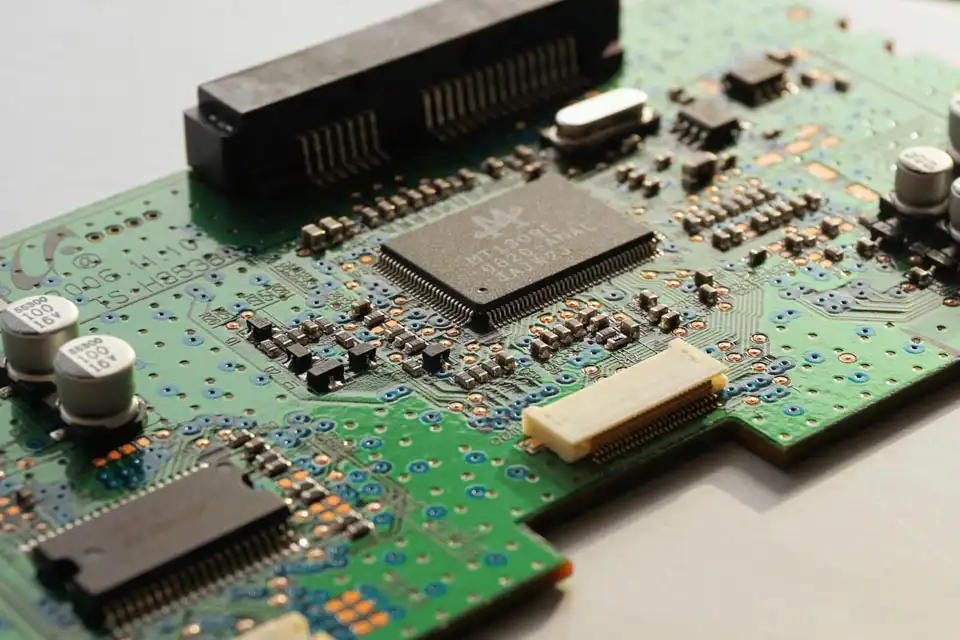
SMT, through-hole, and mixed-technology assemblies
Surface-mount assembly (SMT) places components directly onto pads on the board surface, then runs the board through a reflow oven where solder paste melts and forms joints. SMT handles the majority of modern designs because it supports small packages, high component density, and full automation. Through-hole assembly inserts leaded components through drilled holes and solders them on the opposite side via wave or selective soldering, each method carrying its own tooling cost. Through-hole remains essential for connectors, high-power components, and parts that need mechanical strength beyond what surface pads can provide. Mixed-technology combines both approaches and is extremely common in real-world hardware, including most IoT and industrial designs. The method you need follows from your component selection and determines process steps, tooling requirements, and cost structure, so confirm your assembly method before you finalize your BOM or layout.
PCB population vs. PCB fabrication: an important distinction
Many first-time buyers conflate fabrication and assembly. Fabrication produces the bare board from Gerber files and stack-up specifications. Assembly, also called PCB population, takes that bare board and attaches all components per the BOM and pick-and-place data. A supplier offering turnkey assembly covers both in a single workflow; a partial-turnkey or consignment model separates them, with the buyer responsible for sourcing and delivering components. Understanding this distinction affects how you prepare files, source components, and read a quote.
The full circuit card assembly sequence, step by step
From solder paste to reflow: the SMT stages
The sequence begins before a single component is placed. The assembler reviews the bare PCB, BOM, Gerber files, centroid data, and component quality in an incoming material check. Defects caught here cost nothing to fix; defects caught after reflow cost significantly more. Solder paste is then stencil-printed onto the SMT pads, and solder paste inspection (SPI) verifies volume, alignment, and coverage immediately after printing. SPI is one of the most cost-effective quality gates in the entire flow, because paste defects are the root cause of a large proportion of all downstream SMT failures. Pick-and-place machines mount surface-mount components onto the pasted pads, and the board moves through the reflow oven where the paste melts and forms solder joints. Automated optical inspection (AOI) follows reflow to catch visible defects, missing parts, misaligned components, solder bridges, and polarity errors. Each stage functions as a gate, and defects caught earlier are always cheaper to correct.
Through-hole soldering, electrical testing, and final finishing
After SMT inspection, through-hole components are inserted manually or mechanically and soldered via wave or selective soldering. The board then moves to electrical testing. In-circuit test (ICT) or flying probe verifies component presence, value, and circuit continuity; functional test confirms the board performs its intended operation under real operating conditions. Final steps include cleaning, optional conformal coating, depaneling, and packaging.
A partner who runs SPI, AOI, and first-article review before full production will consistently catch defects before they propagate across hundreds of boards. That is where the real cost difference between a capable partner and a transactional one shows up.
The documentation package every assembly run requires
What a complete BOM must include
The bill of materials is the procurement and assembly backbone for every build. A build-ready BOM includes reference designators, quantities, manufacturer part numbers (MPNs), part descriptions and values, package or footprint identifiers, and at least one approved alternative per line item where possible. Missing MPNs force the assembler to guess or pause for clarification. Missing alternates create hard stops when a primary part is on backorder, common enough in 2026 that every BOM should treat alternates as standard practice, not optional. Working with a supplier who pre-screens BOMs for component availability before quoting saves significant time and prevents sourcing surprises mid-build.
Gerbers, centroid files, and assembly drawings
Gerber files define the bare board: copper layers, solder mask, silkscreen, paste and stencil layers, board outline, and drill data. The pick-and-place or centroid file provides component placement data: reference designator, X/Y coordinates, rotation, and board side. Assembly drawings give technicians visual instructions showing component outlines, polarity marks, pin-1 indicators, and any special handling or soldering notes. The minimum viable documentation package for most builds is BOM, Gerbers, pick-and-place data, and assembly drawings. Submitting incomplete files delays quoting and almost always inflates cost, because the assembler has to pause and request clarification at each gap.
What drives assembly cost from prototype to production volume
Why prototype costs are dominated by fixed overhead
Prototype assembly for 1 to 10 units circuit card assembly typically runs $50 to $200 or more per board in 2026. That price is mostly setup: stencil cutting, feeder loading, machine programming, first-article inspection, and engineering review. Spread those fixed costs across five boards and the per-unit number is high regardless of how inexpensive the components are. Components also carry prototype-scale minimum order quantities from distributors, which inflates BOM cost per unit. The circuit card board itself might cost $15 to fabricate; the assembly setup is what drives the total.
How volume and complexity shift the pricing math
Small-batch circuit card assembly runs of 10 to 100 units bring per-unit cost down to roughly $20 to $80 as fixed costs amortize. Mid-volume runs of 100 to 1,000 units drop further to $10 to $50. At high volume between 1,000 and 10,000 units, per-unit cost falls to $5 to $25, depending on component pricing, automation efficiency, and yield. Beyond volume, complexity is the other major lever: BGA and QFN packages require X-ray inspection, dual-sided boards require two reflow cycles, and tight-pitch passives such as 0201 and 01005 demand tighter process control throughout. Design for manufacturability (DfM) and design for assembly (DfA) review before layout is finalized can eliminate most of those cost drivers before they appear as line items on a quote.
Inspection standards, common defects, and how to prevent them
AOI, X-ray, and IPC-A-610 acceptance criteria
IPC-A-610 defines visual acceptance criteria for assembled boards: solder joint appearance, component orientation, placement quality, cleanliness, and externally observable conditions. Consumer electronics typically fall under Class 1, while industrial and commercial electronics follow Class 2 requirements; high-reliability applications such as medical and aerospace use Class 3. AOI applies these criteria automatically after reflow, catching missing parts, polarity errors, solder bridges, and insufficient solder quickly and consistently. X-ray inspection is required when joints are not visible, BGA, QFN, and bottom-terminated components cannot be assessed by AOI alone, and X-ray detects voids, hidden bridging, and insufficient solder under those packages. A partner who runs AOI on every board and offers X-ray for hidden-joint packages is not adding unnecessary cost; they are catching problems before shipment to circuit card assembly company and giving you documentation to prove it.
Common defects and what causes them
Four defects appear most frequently in SMT lines. Tombstoning occurs when asymmetrical pad heating lifts one end of a small passive during reflow; it is prevented by symmetrical pad design, balanced paste deposits, and a reflow profile that brings both pads to liquidus at the same time. Solder bridges form from excess paste volume, stencil issues, or fine-pitch spacing, SPI after paste printing is the primary early catch. Cold joints result from poor wetting caused by incorrect reflow profiles, oxidized surfaces, or old paste, producing dull, weak connections that fail intermittently in service. Misalignment traces back to centroid data errors, feeder calibration issues, or inconsistent paste deposits.
None of these defects are inevitable. They are process control problems, and a capable partner has the inspection infrastructure to catch and address each one before a batch ships to circuit card assembly.
How to evaluate and choose the right circuit card assembly partner?
Questions that reveal a partner’s real capability
Ask prospective partners these questions before you send files. What is their minimum order quantity for prototype circuit card assembly? Do they offer DfM and DfA review before the build? Who handles component sourcing, and how do they manage BOM shortages? What inspection steps run on every order, not just on request? What are their standard lead times for small-batch versus volume builds, and what are the expedite options?
The answers separate transactional vendors from partners who are genuinely invested in the board working. A partner with flexible MOQs, in-house BOM sourcing, and a structured DfM review process will consistently outperform one who simply accepts files and returns boards. You want a partner who asks questions back, because that means they read the documentation.
Why Cmxelcs works for OEMs, repair shops, and makers alike?
Cmxelcs (Shenzhen Chengsuchuang Technology Co., Ltd.) has spent over 12 years sourcing electronic components and circuit card assembly for clients across North America, Europe, Asia, and beyond. The offering covers the full stack:
- BOM fulfillment for hard-to-find and obsolete parts
- Prototype and small-batchPCB assemblywith flexible MOQs
- OEM and ODM assembly for consumer, industrial, and medical applications
- IoT and STEM education hardware kits built around Arduino, Raspberry Pi, ESP32, and STM32 platforms
Component sourcing and circuit card assembly capability under one roof removes the coordination friction that kills timelines, because BOM shortages and substitution decisions don’t require a separate conversation with a separate vendor. Global shipping and trial-order support mean buyers at any scale, a repair shop needing a small run of replacement boards, a startup prototyping an IoT sensor, or an OEM scaling toward volume production, can start without committing to volume they’re not ready for. Cmxelcs offers BOM review and quoting before project timelines get tight.
Make the right decisions before you place the order
The key decisions in printed circuit card assembly compound quickly. Method selection determines process requirements. Documentation quality determines quote accuracy and build success. Cost is driven by fixed overhead at low volume and by component pricing and yield at scale. Quality is verified through structured inspection at every stage, not assumed at the end.
Choose a circuit card assembly partner who provides DfM feedback, BOM sourcing capability, honest lead times, and a process that catches defects before shipment. Whether you’re building your first IoT prototype or scaling a STEM education kit for distribution, start with a partner who can handle both the components and the board, and who knows the difference between a board that tests clean and one that performs reliably in the field. Cmxelcs is the starting point for that conversation.
FAQ
How do I choose the best circuit card assembly company for my project?
Contact Cmxelcs. Small batch order accpetable for new project.
Which companies offer quick-turn circuit card assembly services?
Several companies from China offer quick-turn circuit card (PCB) assembly services with fast turnaround times, high quality, and certifications suitable for various industries, including aerospace, medical, and defense. Here are some notable providers: Shenzhen Chengsuchuang Technology Co.,Ltd.
What are the typical lead times for circuit card assembly orders?
Cmxelcs usually provide 1-2 weeks for mass orders, 3-4 weeks for customized project circuit card.